The attached zip file was prepared for me by Martin di Federico. It exercises the DAC and ADC channel by copying the bits read from an ADC to the DAC. After following his instruction, I input square wave pulses to ADC_D and read from DAC_A. I see about 340 nSec latency.
You do NOT neet to comile the project, but just copy these files to your 4x2 board and run the notebook:
4x2_echo.bit 4x2_echo.hwh echo_test.ipynb
We'll continue working from this design to see how the latency could be reduced. The RFSoC data converter has many options to explore. In an online forum this is expected:
ADC maximum configuration i.e 8x decimation , NCO enabled and QMC enabled = 103ns (412 sample clocks)
DAC maximum configuraion i.e 8xinterpolation , inverse sync . NCO, QMC enabled = 119ns (760 sample clocks)
That looks like a total of 103+119=222 nSec but I measure 340 nSec.
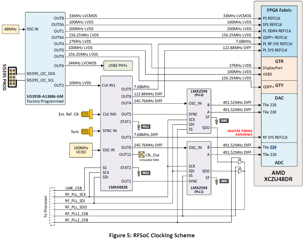
Here is Martin's description of the design, reference 4x2-timing.png also attached.
Hi Chris.
I have create a project and change some stuff..
I create a project and an automated script to create it.
- To open it you should
- Unzip the file
- Open vivado and cd to the unzipped directory
- Run the proj_4x2_echo script from Vivado 2022.1 with the command > source ./proj_4x2_echo.tcl
I will summarize
- I Modified the ADC and DAC Sample Rate
- The sample rate must be a value derivate from the possible clock inputs. In the 4x2 board the clock comes from the LMX chip. The possible frecuencis are 102.4, 204.8, 409.6, 491.52, 737.0.
- I select 491.52Mhz for the clock, and the Sample rate will be 4.9152Gsps.
- I add the reset to the clock signals
- We are using the DAC_A and the ADC_D
- I add a register slice from the input to the output, to make it easier for the Implementation to comply with the timing.
- I add a GPIO to turn ON and OFF the white leds.
- I write a program in python that load the bit file and configure the Clocks.
- echo_test.ipynb

I've repeated this measurement with our SoC and get the same value of 340 ns for the delay. Attached is an oscilloscope trace of the pulse in red and the echo in blue.
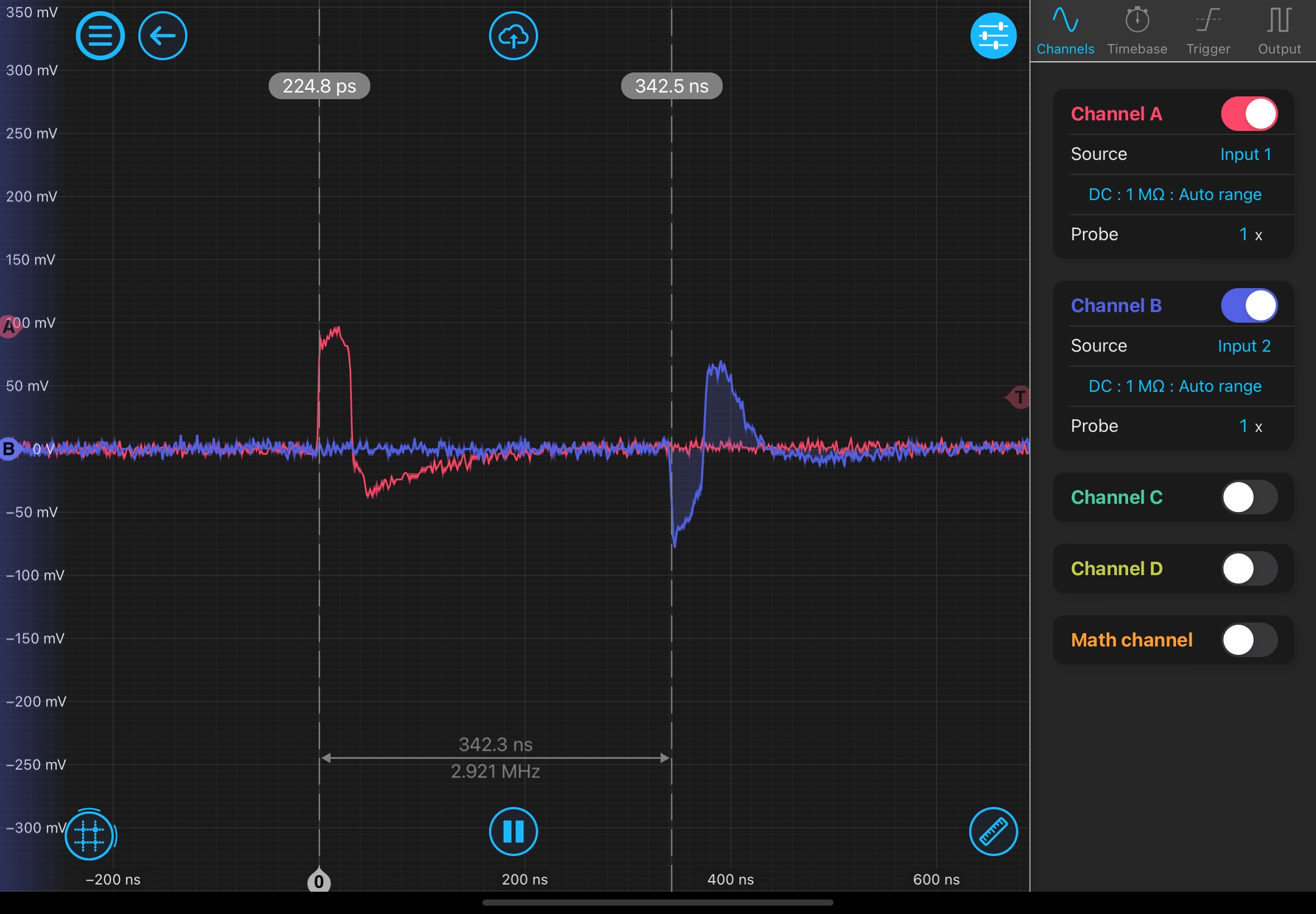
I also performed a swept sin measurement of this same bit file, from 15MHz to 20MHz. The phase info is consistent with a 350 ns delay. Notably the magnitude of the returning sin wave is about half of the one sent in.